- 您现在的位置:买卖IC网 > Sheet目录3875 > PIC18F44J10-I/ML (Microchip Technology)IC PIC MCU FLASH 8KX16 44QFN
PIC16F8X
1998 Microchip Technology Inc.
DS30430C-page 21
5.0
I/O PORTS
The PIC16F8X has two ports, PORTA and PORTB.
Some port pins are multiplexed with an alternate func-
tion for other features on the device.
5.1
PORTA and TRISA Registers
PORTA is a 5-bit wide latch. RA4 is a Schmitt Trigger
input and an open drain output. All other RA port pins
have TTL input levels and full CMOS output drivers. All
pins have data direction bits (TRIS registers) which can
configure these pins as output or input.
Setting a TRISA bit (=1) will make the corresponding
PORTA pin an input, i.e., put the corresponding output
driver in a hi-impedance mode. Clearing a TRISA bit
(=0) will make the corresponding PORTA pin an output,
i.e., put the contents of the output latch on the selected
pin.
Reading the PORTA register reads the status of the pins
whereas writing to it will write to the port latch. All write
operations are read-modify-write operations. So a write
to a port implies that the port pins are first read, then this
value is modified and written to the port data latch.
The RA4 pin is multiplexed with the TMR0 clock input.
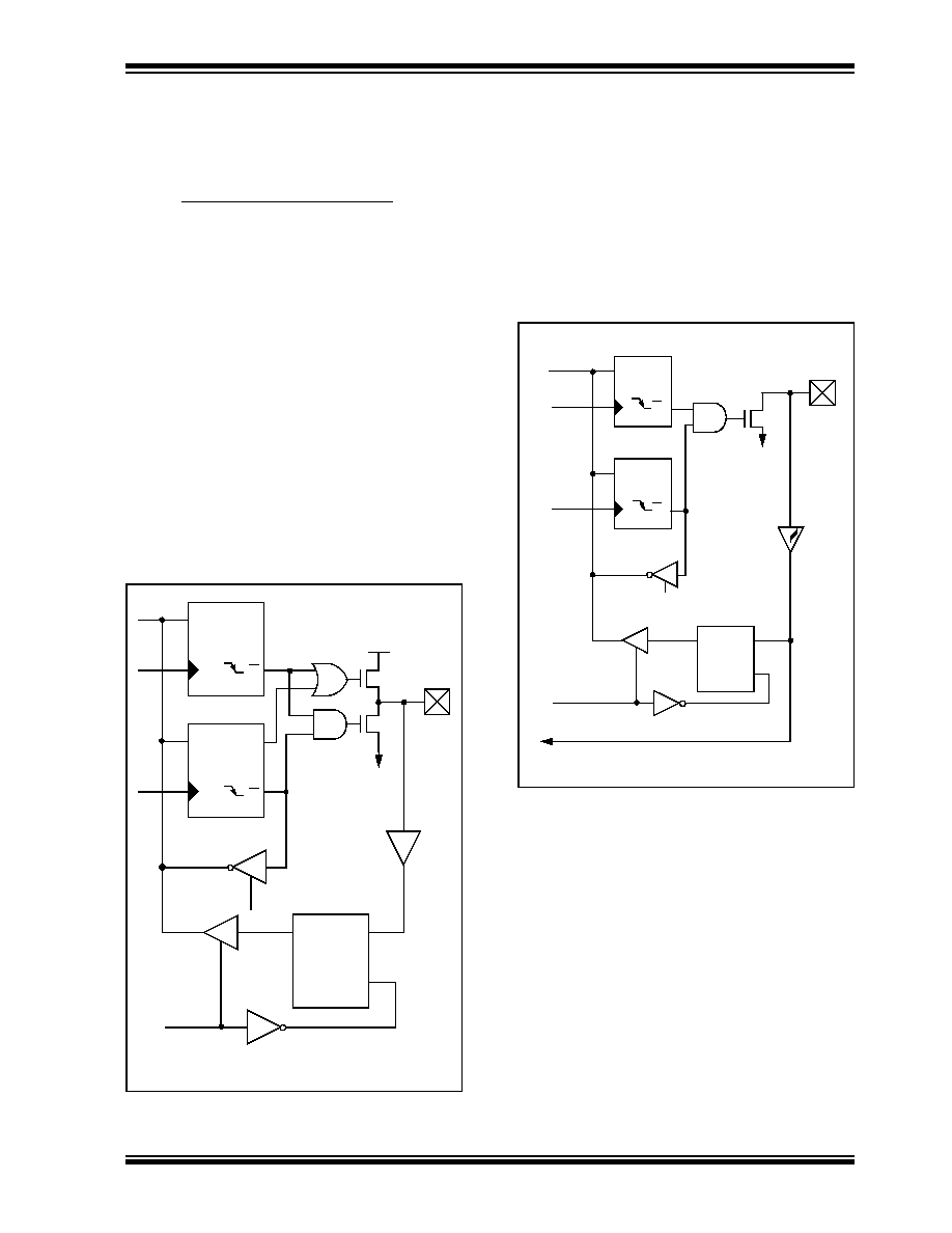
FIGURE 5-1:
BLOCK DIAGRAM OF PINS
RA3:RA0
EXAMPLE 5-1:
INITIALIZING PORTA
CLRF
PORTA
; Initialize PORTA by
; setting output
; data latches
BSF
STATUS, RP0
; Select Bank 1
MOVLW
0x0F
; Value used to
; initialize data
; direction
MOVWF
TRISA
; Set RA<3:0> as inputs
; RA4 as outputs
; TRISA<7:5> are always
; read as ’0’.
FIGURE 5-2:
BLOCK DIAGRAM OF PIN RA4
Note: I/O pins have protection diodes to VDD and VSS.
Data
bus
Q
D
Q
CK
Q
D
Q
CK
QD
EN
P
N
WR
Port
WR
TRIS
Data Latch
TRIS Latch
RD TRIS
RD PORT
TTL
input
buffer
VSS
VDD
I/O pin
Data
bus
WR
PORT
WR
TRIS
RD PORT
Data Latch
TRIS Latch
RD TRIS
Schmitt
Trigger
input
buffer
N
VSS
RA4 pin
TMR0 clock input
Note: I/O pin has protection diodes to VSS only.
Q
D
Q
CK
Q
D
Q
CK
EN
QD
EN
发布紧急采购,3分钟左右您将得到回复。
相关PDF资料
PIC16F628A-I/P
IC MCU FLASH 2KX14 EEPROM 18DIP
PIC18F24K22-I/SO
IC PIC MCU 16KB FLASH 28SOIC
PIC18F23K22-I/SP
IC PIC MCU 8KB FLASH 28SPDIP
PIC18LF23K22-I/SP
IC PIC MCU 8KB FLASH 28SPDIP
PIC24F08KA102-I/SS
IC PIC MCU FLASH 8K 28-SSOP
PIC16C58B-20/SO
IC MCU OTP 2KX12 18SOIC
PIC12C672-04/SM
IC MCU OTP 2KX14 A/D 8-SOIJ
PIC18F25K20-E/SS
IC PIC MCU FLASH 16KX16 28-SSOP
相关代理商/技术参数
PIC18F44J10-I/P
功能描述:8位微控制器 -MCU 16 KB FL 1024 RAM RoHS:否 制造商:Silicon Labs 核心:8051 处理器系列:C8051F39x 数据总线宽度:8 bit 最大时钟频率:50 MHz 程序存储器大小:16 KB 数据 RAM 大小:1 KB 片上 ADC:Yes 工作电源电压:1.8 V to 3.6 V 工作温度范围:- 40 C to + 105 C 封装 / 箱体:QFN-20 安装风格:SMD/SMT
PIC18F44J10-I/PT
功能描述:8位微控制器 -MCU 16 KB FL 1 KB RAM RoHS:否 制造商:Silicon Labs 核心:8051 处理器系列:C8051F39x 数据总线宽度:8 bit 最大时钟频率:50 MHz 程序存储器大小:16 KB 数据 RAM 大小:1 KB 片上 ADC:Yes 工作电源电压:1.8 V to 3.6 V 工作温度范围:- 40 C to + 105 C 封装 / 箱体:QFN-20 安装风格:SMD/SMT
PIC18F44J10T-I/ML
功能描述:8位微控制器 -MCU 16 KB FL 1024 RAM RoHS:否 制造商:Silicon Labs 核心:8051 处理器系列:C8051F39x 数据总线宽度:8 bit 最大时钟频率:50 MHz 程序存储器大小:16 KB 数据 RAM 大小:1 KB 片上 ADC:Yes 工作电源电压:1.8 V to 3.6 V 工作温度范围:- 40 C to + 105 C 封装 / 箱体:QFN-20 安装风格:SMD/SMT
PIC18F44J10T-I/PT
功能描述:8位微控制器 -MCU 16 KB FL 1024 RAM RoHS:否 制造商:Silicon Labs 核心:8051 处理器系列:C8051F39x 数据总线宽度:8 bit 最大时钟频率:50 MHz 程序存储器大小:16 KB 数据 RAM 大小:1 KB 片上 ADC:Yes 工作电源电压:1.8 V to 3.6 V 工作温度范围:- 40 C to + 105 C 封装 / 箱体:QFN-20 安装风格:SMD/SMT
PIC18F44J11-I/ML
功能描述:8位微控制器 -MCU 16KB Flash 4KBRAM 12MIPS nanoWatt RoHS:否 制造商:Silicon Labs 核心:8051 处理器系列:C8051F39x 数据总线宽度:8 bit 最大时钟频率:50 MHz 程序存储器大小:16 KB 数据 RAM 大小:1 KB 片上 ADC:Yes 工作电源电压:1.8 V to 3.6 V 工作温度范围:- 40 C to + 105 C 封装 / 箱体:QFN-20 安装风格:SMD/SMT
PIC18F44J11-I/PT
功能描述:8位微控制器 -MCU 16KB Flash 4KBRAM 12MIPS nanoWatt RoHS:否 制造商:Silicon Labs 核心:8051 处理器系列:C8051F39x 数据总线宽度:8 bit 最大时钟频率:50 MHz 程序存储器大小:16 KB 数据 RAM 大小:1 KB 片上 ADC:Yes 工作电源电压:1.8 V to 3.6 V 工作温度范围:- 40 C to + 105 C 封装 / 箱体:QFN-20 安装风格:SMD/SMT
PIC18F44J11T-I/ML
功能描述:8位微控制器 -MCU 16KB Flash 4KBRAM 12MIPS nanoWatt RoHS:否 制造商:Silicon Labs 核心:8051 处理器系列:C8051F39x 数据总线宽度:8 bit 最大时钟频率:50 MHz 程序存储器大小:16 KB 数据 RAM 大小:1 KB 片上 ADC:Yes 工作电源电压:1.8 V to 3.6 V 工作温度范围:- 40 C to + 105 C 封装 / 箱体:QFN-20 安装风格:SMD/SMT
PIC18F44J11T-I/PT
功能描述:8位微控制器 -MCU 16KB Flash 4KBRAM 12MIPS nanoWatt RoHS:否 制造商:Silicon Labs 核心:8051 处理器系列:C8051F39x 数据总线宽度:8 bit 最大时钟频率:50 MHz 程序存储器大小:16 KB 数据 RAM 大小:1 KB 片上 ADC:Yes 工作电源电压:1.8 V to 3.6 V 工作温度范围:- 40 C to + 105 C 封装 / 箱体:QFN-20 安装风格:SMD/SMT